 | –≠–ª–µ–∫—Ç—Ä–æ–Ω–Ω—ã–π –∫–æ–º–ø–æ–Ω–µ–Ω—Ç: STK4042 | –°–∫–∞—á–∞—Ç—å:  PDF PDF  ZIP ZIP |
Thick Film Hybrid IC
Ordering number : EN4390A
N3096HA (OT)/31993YO 5-2171 No. 4390-1/5
SANYO Electric Co.,Ltd. Semiconductor Bussiness Headquarters
TOKYO OFFICE Tokyo Bldg., 1-10, 1 Chome, Ueno, Taito-ku, TOKYO, 110 JAPAN
AF Power Amplifier (Split Power Supply)
(80 W min, THD = 0.08%)
STK4042V
Features
∑ Compact packaging supports slimmer set designs
∑ Series designed from 20 up to 100 W (200 W) and pin-
compatibility (120 to 200 W have 18 pins)
∑ Simpler heat sink design facilitates thermal design of
slim stereo sets
∑ Current mirror circuit application reduces distortion to
0.08%
∑ Supports addition of electronic circuits for thermal
shutdown and load-short protection circuit as well as
pop noise muting which occurs when the power supply
switch is turned on and off
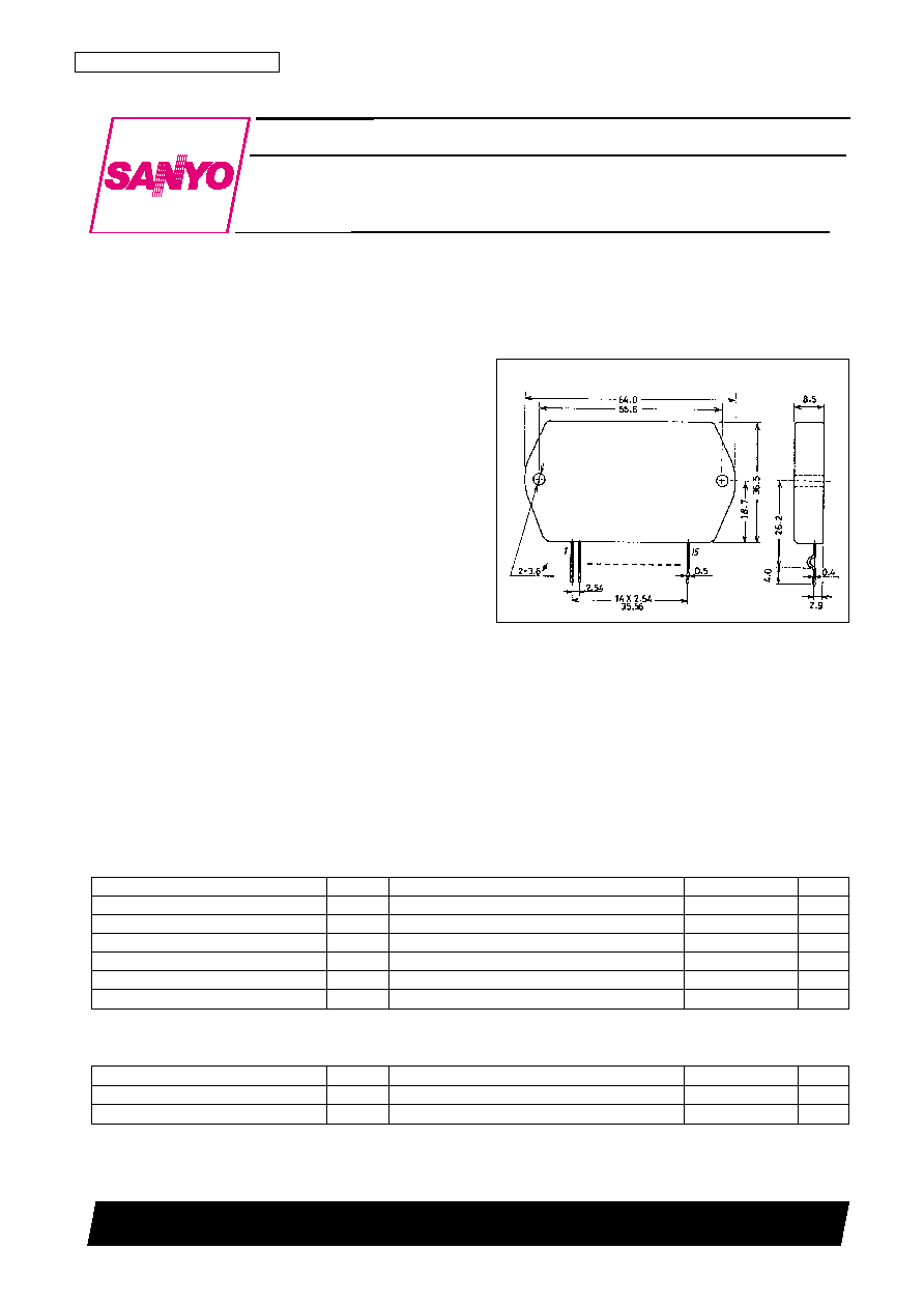
Package Dimensions
unit : mm
4075
Specifications
Maximum Ratings
at Ta = 25∞C
Recommended Operational Voltage
at Ta = 25∞C
[STK4042V]
Parameter
Symbol
Conditions
Ratings
Unit
Maximum supply voltage
V
CC
max
±65
V
Thermal resistance
j-c
1.2
∞C/W
Junction temperature
Tj
150
∞C
Operating substrate temperature
Tc
125
∞C
Storage temperature
Tstg
≠30 to +125
∞C
Available time for load shorted
ts
*
1
V
CC
= ±45 V, R
L
= 8
, f = 50 Hz, P
O
= 80 W
1
s
Parameter
Symbol
Conditions
Ratings
Unit
Recommended supply voltage
V
CC
±45
V
Load resistance
R
L
8
STK4042V
No. 4390-2/5
Operating Characteristics
at Ta = 25∞C, V
CC
= ±45 V, R
L
= 8
, VG = 40 dB, Rg = 600
, 100k LPF ON, R
L
(non-inductive)
Note: Use rated power supply for test unless otherwise specified.
*
1
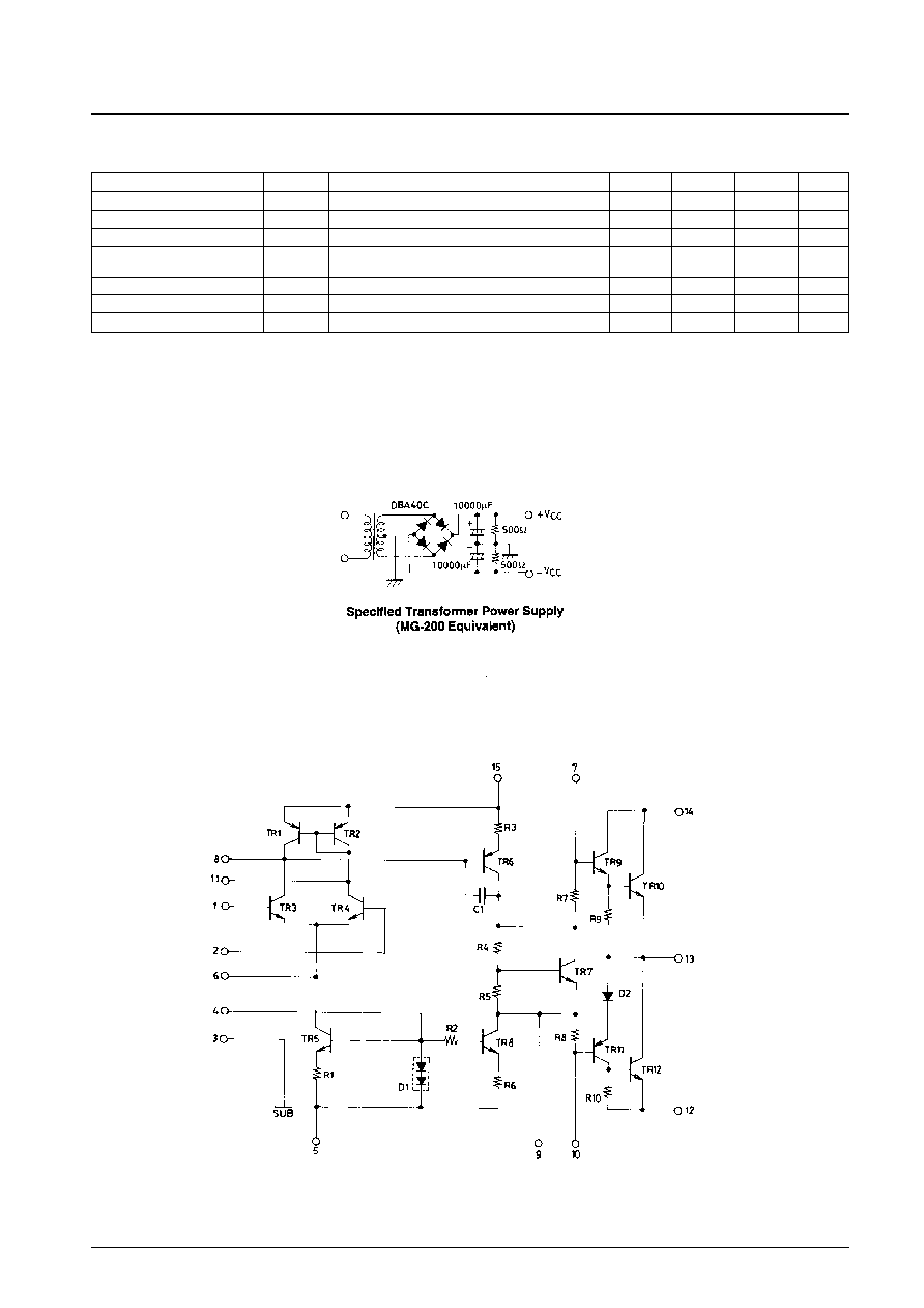
When measuring permissible load short time and output noise voltage use transformer power supply indicated below.
*
2
Output noise voltage represents the peak value on the rms scale (VTVM). The noise voltage waveform does not include the pulse noise.
Equivalent Circuit
Parameter
Symbol
Conditions
min
typ
max
Unit
Quiescent current
I
CCO
V
CC
= ±54 V
15
120
mA
Output power
P
O
(1)
THD = 0.08%, f = 20 Hz to 20 kHz
80
W
Total harmonic distortion
THD
P
O
= 1.0 W, f = 1 kHz
0.08
%
Frequency response
f
L
, f
H
P
O
= 1.0 W,
+0
dB
20 to 50k
Hz
≠3
Input resistance
r
i
P
O
= 1.0 W, f = 1 kHz
55
k
Output noise voltage
V
NO
*
2
V
CC
= ±54 V, R
g
=10 k
1.2
mVrms
Neutral voltage
V
N
V
CC
= ±54 V
≠70
0
+70
mV
STK4042V
No. 4390-3/5
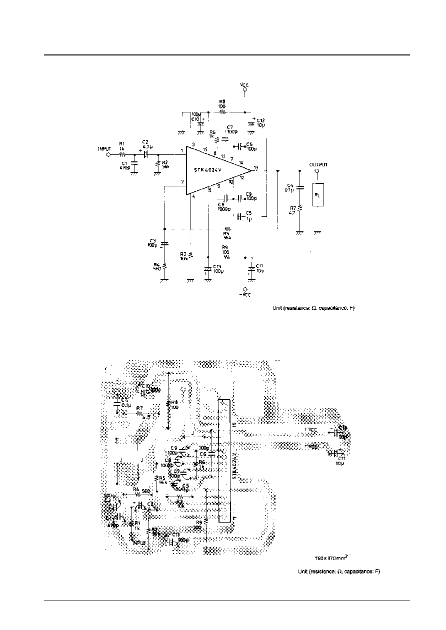
Application Circuit: 80W min Single Channel AF Power Amplifier
Sample Printed Circuit Pattern for Application Circuit (Copper-foiled side)
STK4042V
No. 4390-4/5
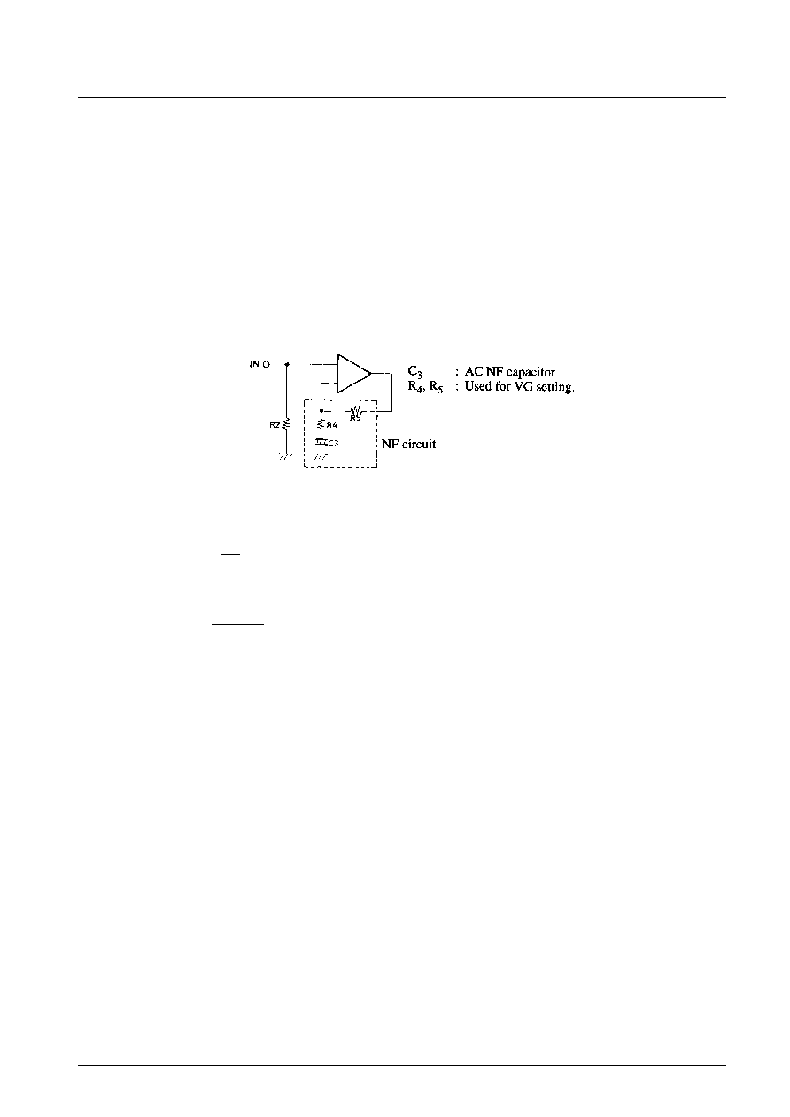
Description of External Parts
R
1
, C
1
: Input filter circuit
∑ Reduces high-frequency noise.
C
2
: Input coupling capacitor
∑ DC current suppression. A reduction in reactance is effective because of increases in capacitor
reactance at low frequencies and 1/f noise dependence on signal source resistance which result in
output noise worsening.
R
2
: Input bias resistor
∑ Biases the input pin to zero.
∑ Effects V
N
stability (refer to NF circuit).
∑ Due to differential input, input resistance is more or less determined by this resistance value.
R
4
, R
5
: NFB circuit (AC NF circuit). Use of resistor with 1% error is suggested.
C
3
(R
2
)
∑ VG settings are obtained using R
4
and R
5
according to the following equation:
log20∑
R
5
40 dB is recommended.
R
4
∑ Low-frequency cutoff frequency settings are obtained using R
4
and C
3
according to the following
equation:
f
L
=
1
[Hz]
2
∑R
4
∑C
3
When changing the VG setting, you should change R
4
which requires a recheck of the low cutoff
frequency setting. When the VG setting is changed using R
5
, the setting should ensure R
2
equals R
5
so
that V
N
balance stability is maintained. If the resistor value is increased more than the existing value,
V
N
balance may be disturbed and result in deterioration of V
N
temperature characteristics.
R
3
: Differential constant-current bias resistor
R
6
, R
7
: For oscillation suppression and phase compensation applications
(For use with differential stage applications)
R
7
, C
4
: For oscillation suppression and phase compensation applications
(A Mylar capacitor is recommended for C
4
for use with output stage applications)
C
6
, C
9
: For oscillation suppression and phase compensation applications
Power stage (Must be connected near the pin)
C
6
: Positive (+) power
C
9
: Negative (≠) power
C
8
: For oscillation suppression and phase compensation applications
(Oscillation suppression before power step clip)
C
5
: For oscillation suppression and distortion improvement applications
R
8
, C
10
: Ripple filter circuit on positive (+) side.
R
9
, C
13
: Ripple filter circuit on negative (≠) side.
C
11
, C
12
: For oscillation suppression applications
∑ Used for reducing power supply impedance to stable IC operation and should be connected near the IC
pin. We recommend that you use an electrolytic capacitor.
R
10
: Output resistor
Increases load shorting endurance capacity during times of high output.
R
14
, L
1
: For oscillation suppression applications
Increases oscillation stability against capacitance loads.

STK4042V
No. 4390-5/5
Sample Application Circuit (Protection circuit and muting circuit)
This catalog provides information as of November, 1996. Specifications and information herein are subject to
change without notice.
s
No products described or contained herein are intended for use in surgical implants, life-support systems, aerospace
equipment, nuclear power control systems, vehicles, disaster/crime-prevention equipment and the like, the failure of
which may directly or indirectly cause injury, death or property loss.
s
Anyone purchasing any products described or contained herein for an above-mentioned use shall:
x
Accept full responsibility and indemnify and defend SANYO ELECTRIC CO., LTD., its affiliates, subsidiaries and
distributors and all their officers and employees, jointly and severally, against any and all claims and litigation and all
damages, cost and expenses associated with such use:
Not impose any responsibility for any fault or negligence which may be cited in any such claim or litigation on
SANYO ELECTRIC CO., LTD., its affiliates, subsidiaries and distributors or any of their officers and employees
jointly or severally.
s
Information (including circuit diagrams and circuit parameters) herein is for example only; it is not guaranteed for
volume production. SANYO believes information herein is accurate and reliable, but no guarantees are made or implied
regarding its use or any infringements of intellectual property rights or other rights of third parties.